How to Hack an Expensive Camera and Not Get Killed by Your Wife
Disclaimer
This research started in 2013, so if you find some of my methods silly and dangerous - you are right, they were. However, I still learnt a lot from the process.
Prologue
It all started several months before my first child was born. My wife and I always wanted a Leica camera and suddenly we realized that if we didn’t buy it now, we will not be able to for a while. So we put in an order for M240 and … bam, backlog for almost half a year. Pretty soon I got bored waiting and started to explore the Leica website. The downloads section caught my attention immediately. Well, you can guess why - firmware images!
Leica firmware files
Leica M8 firmware
It was unencrypted, uncompressed file (m8-2_005.upd) starting with PWAD magic[1]. Does anyone recognise it? Yes you got it right - Doom Patch WAD format. These guys seem to love the classics. The format is very well documented and writing the splitting tool was a pretty simple task to do[2].
It is actually very funny, because later when I was looking into the compressed Leica T firmware, the first thing I did was to check the compression methods used by id Software in the past. Wikipedia says they used LHA[3] which is essentially LZW. But when I tried some generic LZW decompressors it didn’t work, so I started to look for an id Software specific implementation and voila, the one from Catacomb Armageddon source[4] was spot on. I have to admit it was a lucky coincidence.
Anyway, back to M8, this is the firmware structure
RULES:      0x0000008C (    3036:0x00000BDC) - XML description
LUTS:       0x00000C68 (  183274:0x0002CBEA)
 GAMMA:     0x0000007C (   31760:0x00007C10)
 GAIN:      0x00007C8C (   50344:0x0000C4A8)
 LEICA:     0x00014134 (    7000:0x00001B58)
 BLEMISH:   0x00015C8C (     250:0x000000FA)
 WREF:      0x00015D88 (   82480:0x00014230)
 OBJ:       0x00029FB8 (   11268:0x00002C04)
 VERSION:   0x0002CBBC (      46:0x0000002E)
PXA:        0x0002D854 (  858384:0x000D1910)
BF:         0x000FF164 (  134522:0x00020D7A) - Analog Devices Blackfin Processor family
GUI:        0x0011FEE0 ( 3574180:0x003689A4)
 TRANS:     0x0000005C (   59988:0x0000EA54) - localization
 IMAGES:    0x0000EAB0 (  267433:0x000414A9)
  21_1PRT:  0x000000CC (   18411:0x000047EB) - JFIF image
  21_2GRP:  0x000048B8 (   23172:0x00005A84) - JFIF image
  21_3PAN:  0x0000A33C (   23034:0x000059FA) - JFIF image
  24_1PRT:  0x0000FD38 (   18489:0x00004839) - JFIF image
  24_2GRP:  0x00014574 (   23230:0x00005ABE) - JFIF image
  24_3PAN:  0x0001A034 (   22998:0x000059D6) - JFIF image
  28_1PRT:  0x0001FA0C (   22605:0x0000584D) - JFIF image
  28_2GRP:  0x0002525C (   23081:0x00005A29) - JFIF image
  28_3PAN:  0x0002AC88 (   23282:0x00005AF2) - JFIF image
  35_1PRT:  0x0003077C (   22496:0x000057E0) - JFIF image
  35_2GRP:  0x00035F5C (   23532:0x00005BEC) - JFIF image
  35_3PAN:  0x0003BB48 (   22881:0x00005961) - JFIF image
 FONT1:     0x0004FF5C ( 1522988:0x00173D2C)
 FONT2:     0x001C3C88 ( 1723676:0x001A4D1C)
 VERSION:   0x003689A4 (       0:0x00000000)
M16C:       0x00488884 (  130406:0x0001FD66) - Renesas M16C Family (Motorola S-record)
FPGA:       0x004A85EC (  131604:0x00020214) - Xilinx Spartan 3
FSL:        0x004C8800 (     814:0x0000032E) - First Stage Loader
IDA doesn’t support Blackfin processors out of the box, but one third-party plugin does[5].
Leica M9 firmware
This one (m9-1_196.upd) looked encrypted (histogram shows distribution around 0.45%).
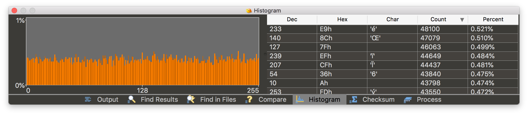
End of story? Maybe not, because Leica used to put pretty weak CPUs in their cameras and XOR encryption was very popular at that time in consumer electronics, so I decided to write a simple XOR manipulation tool to compare the firmware with itself and calculate some statistics along the way.
Key length was determined by looking for the longest repeating pattern. This makes sense since any firmware usually includes big blocks of repeating data like 0x00/0xFF paddings or graphics with LUT pixels. The key itself is calculated based on per byte statistics within key length where most frequently occurring byte goes to key buffer. The output clearly pointed to XOR encryption. Then it was a matter of modifying my tool a bit to get a potential key and decrypt[6]. Yet again, it was PWAD file after decryption.
The PWAD contents revealed the following structure:
RULES:      0x0000007C (    2788:0x00000AE4) - XML description
LUTS:       0x00000B60 ( 4060616:0x003DF5C8)
 PROCESS:   0x0000004C ( 3900572:0x003B849C)
  CREATE:   0x0000004C (      20:0x00000014) - timestamp
  LUTS:     0x00000060 (  427744:0x000686E0)
  GAINMAP:  0x00068740 (   20008:0x00004E28)
  LENS:     0x0006D568 ( 3452724:0x0034AF34)
 CCD:       0x003B84E8 (  148662:0x000244B6)
  CREATE:   0x0000004C (      20:0x00000014) - timestamp
  BLEMISH:  0x00000060 (    1092:0x00000444)
  WREF:     0x000004A4 (  147452:0x00023FFC)
  LIN:      0x000244A0 (      22:0x00000016)
 ICCPROF:   0x003DC9A0 (    4304:0x000010D0)
  ECI-RGB:  0x0000003C (     540:0x0000021C)
  sRGB:     0x00000258 (    3144:0x00000C48)
  A-RGB:    0x00000EA0 (     560:0x00000230)
 WBPARAM:   0x003DDA70 (    7000:0x00001B58)
BF561:      0x003E0128 (  289128:0x00046968) - Analog Devices Blackfin Processor family
 bf0:       0x0000004C (  117846:0x0001CC56) - main processor firmware
 bf1:       0x0001CCA4 (  117826:0x0001CC42) - sub-processor firmware
 bf0.map:   0x000398E8 (   27072:0x000069C0) - main processor firmware map with symbols :D
 bf1.map:   0x000402A8 (   26304:0x000066C0) - sub-processor firmware map with symbols :D
BODY:       0x00426A90 (  143280:0x00022FB0) - Renesas M16C Family (Motorola S-record)
GUI:        0x00449A40 ( 3647624:0x0037A888)
 TRANS:     0x0000005C (  131656:0x00020248) - localization
 IMAGES:    0x000202A4 (  267433:0x000414A9)
  21_1PRT:  0x000000CC (   18411:0x000047EB) - JFIF image
  21_2GRP:  0x000048B8 (   23172:0x00005A84) - JFIF image
  21_3PAN:  0x0000A33C (   23034:0x000059FA) - JFIF image
  24_1PRT:  0x0000FD38 (   18489:0x00004839) - JFIF image
  24_2GRP:  0x00014574 (   23230:0x00005ABE) - JFIF image
  24_3PAN:  0x0001A034 (   22998:0x000059D6) - JFIF image
  28_1PRT:  0x0001FA0C (   22605:0x0000584D) - JFIF image
  28_2GRP:  0x0002525C (   23081:0x00005A29) - JFIF image
  28_3PAN:  0x0002AC88 (   23282:0x00005AF2) - JFIF image
  35_1PRT:  0x0003077C (   22496:0x000057E0) - JFIF image
  35_2GRP:  0x00035F5C (   23532:0x00005BEC) - JFIF image
  35_3PAN:  0x0003BB48 (   22881:0x00005961) - JFIF image
 FONT1:     0x00061750 ( 1522988:0x00173D2C)
 USBLOGO:   0x001D547C (    1775:0x000006EF) - JFIF image
 FONT2:     0x001D5B6C ( 1723676:0x001A4D1C)
FPGA:       0x007C42C8 (  150176:0x00024AA0) - Xilinx Spartan 3A
BF547:      0x007E8D68 (  937576:0x000E4E68) - Analog Devices Blackfin Processor family (FSL?)
Leica M240 firmware
It became a habit to check Leica firmware download page every morning. Eventually a new file became available - FW_M240_1_1_0_2.FW.
It didn’t look encrypted, but it did look compressed…
Compression
The histogram had a huge spike on 0x9D.
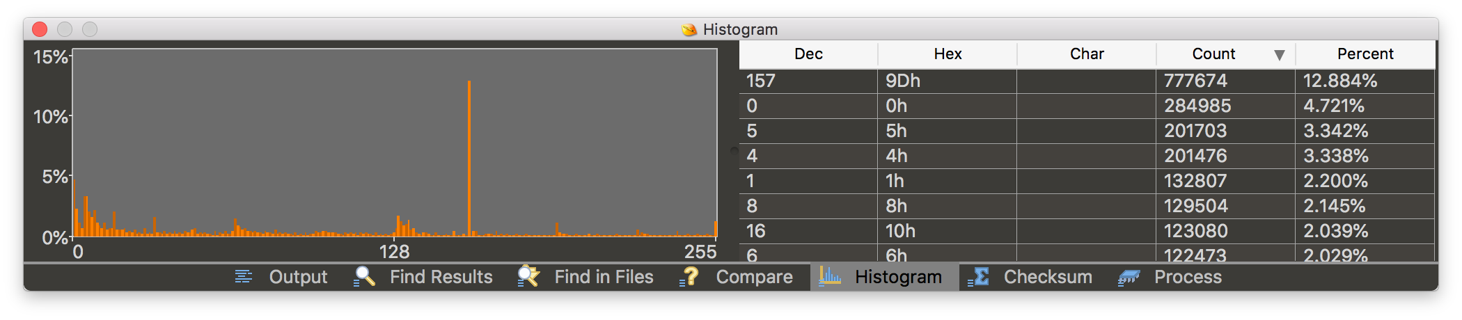
Probably this is some kind of compression magic. Googling for “9D” and “compression” didn’t help apart from the fact that 0x1F9D is used as LZW compression signature[7]. Just in case, I got myself familiar with LZ compression types and decided to look around for all bytes following 0x9D. I found four different patterns:
9D 70 C49D 009D XX YY9D XX 8Y YY
My observations regarding these pattern types were:
- (1) appears once at address 0x30, probably used as compressed data indicator
- XX is never bigger than 0x7F
- last byte YY in (3) and (4) is never bigger than 0x7F
From what I learnt about LZ, it looks a lot like LZ77 or LZSS if YY is the step back distance and XX is the count of bytes to copy. And (2) is a special case to output 0x9D. Writing a simple C function implementing this logic confirmed that it was heading in the right direction, but still not quite there yet because of (4).
I spent some time trying different ways to interpret it, but nothing worked. So I just asked some other folks what they thought and one guy noticed that according to my own observations fourth byte YY appears only when highest bit of 0x8Y is set adding extra length to step back distance. Shame on me, it was so obvious. Finally the decompressor started to output a valid stream… until it stuck somewhere in the middle of the firmware file. This was due to an unknown length of a sliding window. Extra debugging and experiments fixed it.
Then it was time for a new tool to work with M240 firmware files[8].
Firmware structure
To deal an unknown file format, I couldn’t think of anything better than to measure some offsets and sizes in the file and try to find the closest values in the file header. Like this block for example:
0x00: 1E 1C AF 2E 01 01 00 02 07 E1 EA 5E 00 5C 1A B1
0x10: 01 29 1A 7E AE 38 73 65 9C 3D 75 B4 34 2F 44 6E
0x20: 13 17 8E 6B 00 00 00 01 00 00 00 30 E1 E3 50 D1
eventually turned into:
1E1CAF2E - looks like "LEICA FILE"
01010002 - 1.1.0.2
005C1AB1 - compressed file size (big endian)
01291A7E - uncompressed file size (big endian)
AE3873659C3D75B4342F446E13178E6B - MD5 hash
00000001 - number of payloads
00000030 - first payload offset
The tool was growing along with better understanding of firmware structures and eventually the output looked like this:
Running with options:
  + firmware folder: M240_FIRMWARE
  + verbose enabled

Open firmware file: FW_M240_1_1_0_2.FW
  File size:  6036193 | 0x005C1AE1

Parse container header:
  version:       1.1.0.2
  packed size:    6036145 | 0x005C1AB1
  unpacked size: 19470974 | 0x01291A7E
  body blocks:          1 | 0x00000001
  body offset:         48 | 0x00000030
  MD5:           AE387365 9C3D75B4 342F446E 13178E6B
  MD5 check:     PASSED

Uncompress container body: ◼◼◼◼◼◼◼◼◼◼◼◼◼◼◼◼◼◼◼◼◼◼◼◼◼◼
  6036145 -> 19470974
  Uncompression: DONE

Split container:
  Number of sections:          9 | 0x00000009
  Section table size:        612 | 0x00000264
  Section table offset:       36 | 0x00000024
  Section 1
    Section Name:   "[A]IMG_LOKI-212"
    Section offset:        0 | 0x00000000
    Section size:    7340032 | 0x00700000
    Section base:    1048576 | 0x00100000
    MD5:            A8D55AA2 B0ACDB14 0673AD79 707674F3
    MD5 check:      PASSED
    Create file:    M240_FIRMWARE/IMG_LOKI-212.bin

  ~~~~~~~~~~~~~~~~~~~~~~~~~~~~~~~~~~~~~~~~~~~~~~~~

  Section 9
    Section Name:   "[A]IMG-LENSDATA-213"
    Section offset: 19214844 | 0x012531FC
    Section size:     255478 | 0x0003E5F6
    Section base:   16252928 | 0x00F80000
    MD5:            39C2BEC0 27ED23F6 2C1C8513 EEE697B9
    MD5 check:      PASSED
    Create file:    M240_FIRMWARE/IMG-LENSDATA-213.bin
  Splitting container: DONE
Extraction COMPLETE!
M240 firmware includes one container with 9 items:
IMG_LOKI-212.bin     - Application Processor Firmware
IMG_LOKI-213.bin     - Application Processor Firmware
CTRL_SYS-11.bin      - IO Processor Firmware
IMG-FPGA-212.bin     - Image Processing (Sensor) Firmware
IMG-FPGA-213.bin     - Image Processing (Sensor) Firmware
IMG-DSP-212.bin      - DSP Firmware
IMG-DSP-213.bin      - DSP Firmware
IMG-LENSDATA-212.bin - Lens Data
IMG-LENSDATA-213.bin - Lens Data
As you have noticed there are two sets of files in one firmware. Later I found out that 212 is an Image Board version meant that there were two different Leica M240 types in the wild. The current research is based on 212 one.
System Control - CTRL_SYS-11.bin
The only common part was the firmware for some system control chip. This binary actually has lots of strings and looking through them it is not hard to get an idea what this part is for.
$ strings CTRL_SYS-11.bin | rg SH
-> Test SH7216 data flash driver
-> Test SH7216 SCI driver
-> Test SH7216 I2C driver
-> Test SH7216 MTU2 driver
-> Test SH7216 ADC functions
-> Test SH7216 CMT driver
So this is a Renesas SH7216 (SH-2A) and it is responsible for early boot stage, IO tests and firmware update.
IDA supports this processor type out of the box, so it was a matter of finding the correct image base which was known from the firmware section description - 0x0:
Section Name:   "[A]CTRL_SYS-11"
Section offset: 14680064 | 0x00E00000
Section size:     917277 | 0x000DFF1D
Section base:          0 | 0x00000000
I have obviously put it into IDA and recognised all functions, but didn’t really dig into it much since I was lot more curious about the main processor firmware.
Another thing to note here is that UART from this chip is exposed on service port where it prints boot log. We will get back to that later.
Main Chip - IMG_LOKI-212.bin
In order to start reverse engineering this firmware it was necessary to answer several questions first:
- what is the processor type
- what is the image base
- what OS it is based on if any
We already know image base from the M240FwTool, it is 0x100000
Section Name:   "[A]IMG_LOKI-212"
Section offset:        0 | 0x00000000
Section size:    7340032 | 0x00700000
Section base:    1048576 | 0x00100000
Answers to the remaining questions were stored inside the firmware in human readable form. This string for example:
$ strings ./IMG_LOKI-212.bin | rg Softune
6Softune REALOS/FR is Realtime OS for FR Family, based on micro-ITRON COPYRIGHT(C) FUJITSU LIMITED 1994-1999
...
So we are dealing with custom Fujitsu FR (Leica calls it Maestro) and Softune REALOS. Actually, it was a lot more promising than Blackfin because IDA provides FR support out of the box.
IDA FR processor module
Reality was not that bright though, because when I put the firmware file into IDA and chose FR processor I discovered that this module is barely usable due to missing instructions, absence of xrefs etc.
I decided to fix it but ended up rewriting some parts completely[9]. This is the result:
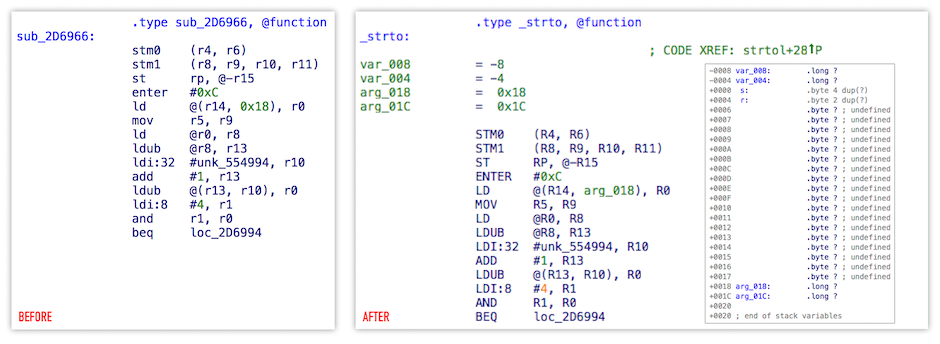
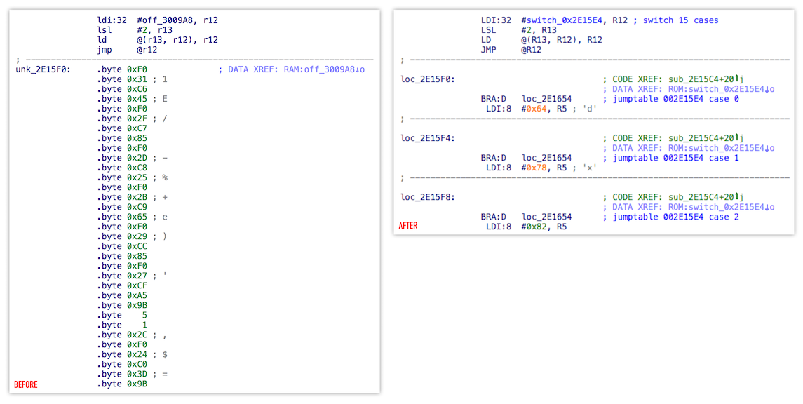
Apart from fixes in ana, ins and out stages, brand new emu code was able to
- recognize various types of code and data xrefs
- recognize switch statements
- perform stack trace
- split stack arguments and local variables (thanks to clean FR ABI)
- recognise functions properly
But the biggest change as you have noticed was capital letters for instructions :)
Would you like to see the full instruction set?
Here it is:
    ADD      OR       BTSTH    LSR     MOV     BN       LDRES     EXTSH
    ADD2     ORH      MUL      LSR2    JMP     BP       STRES     EXTUH
    ADDC     ORB      MULU     ASR     CALL    BV       COPOP     SRCH0
    ADDN     EOR      MULH     ASR2    RET     BNV      COPLD     SRCH1
    ADDN2    EORH     MULUH    LDI     INT     BLT      COPST     SRCHC
    SUB      EORB     DIV0S    LDI     INTE    BGE      COPSV     LDM0
    SUBC     BANDL    DIV0U    LDI     RETI    BLE      NOP       LDM1
    SUBN     BANDH    DIV1     LD      BRA     BGT      ANDCCR    STM0
    CMP      BORL     DIV2     LDUH    BNO     BLS      ORCCR     STM1
    CMP2     BORH     DIV3     LDUB    BEQ     BHI      STILM     ENTER
    AND      BEORL    DIV4S    ST      BNE     DMOV     ADDSP     LEAVE
    ANDH     BEORH    LSL      STH     BC      DMOVH    EXTSB     XCHB
    ANDB     BTSTL    LSL2     STB     BNC     DMOVB    EXTUB
That’s it, nice and simple.
By the way, you may have noticed that some instructions are not aligned:
   BRA:D    loc_xxx
    LDI:8   #0x64, R5
It is not a bug in a processor module, but actually a feature of Fujitsu FR family. It is called “Delay Slot”[10] and quite typical for RISC processors.
From the FR80 hardware manual[11]:
The instruction that is located immediately following a branch instruction (the location is called a
"delay slot") is executed before branching, and an instruction at the branch destination is executed
after that. Because the instruction in the delay slot is executed before the branch operation, the
apparent execution speed is 1 cycle.
So this is essentially a pipeline optimisation and it is better to keep that in mind since it is used everywhere in Leica firmware.
Softune REALOS
From wiki[12]:
Softune is an Integrated development environment from Fujitsu for the Fujitsu FR, FR-V and F²MC
processor families. It provides an REALOS µITRON realtime kernel.
It is for example used for Nikon DSLRs (see Nikon EXPEED) and some Pentax K mount cameras.
So it is quite a popular decent RTOS with tasks, semaphores and other goodies and I was wondering if it is possible to recognize some standard library functions in the Leica firmware.
FLIRT
I should have called this part “an ode to time wasting” and here is why.
It was pretty hard to find Softune IDE in the wild but eventually I managed to get something to play with. As expected the IDE included libraries. There were four binaries:
- lib911.lib
- lib911e.lib
- lib911if.lib
- lib911p.lib
I don’t know why, but maybe by inertia, since I was so into hacking everything related to Leica but I have actually started to reverse engineer object format. Yes very well documented Object Module Format[13]. And yes of course I wrote a tool to deal with it[14]:
Fujitsu RISC Library Tool v1.0
Usage: FRLibTool [-s start] [-i imagebase] [-o output] [-f index] [-dv] FIRMWARE.BIN LIBRARY.LIB

This tool will help you to find Softune REALOS library functions in FR (Fujitsu RISC) firmware.
Use following arguments:
    -f       Specify firmware image file
    -s       Specify firmware image scan offset
    -b       Specify firmware imagebase
    -o       Specify output type (exclusively)
       list  - list of functions
       idc   - IDC script
       py    - IDA python script
       pat   - FLAIR pattern file
    -i xxx   Specify index of particular function
    -d       Dump library
    -v       Be verbose
Using this tool it was possible to create *.pat files and use them as input for the IDA FLAIR tool to generate signature files[15].
$ FRLibTool -o pat lib911.lib
$ FRLibTool -o pat lib911e.lib
$ FRLibTool -o pat lib911if.lib
$ FRLibTool -o pat lib911p.lib
...
$ sigmake -n "SOFTUNE C/C++ Library" lib911.pat lib911e.pat lib911if.pat lib911p.pat softune.sig
Finally, after applying this signature, I was very pleased to see matches in IMG_LOKI-212.idb .
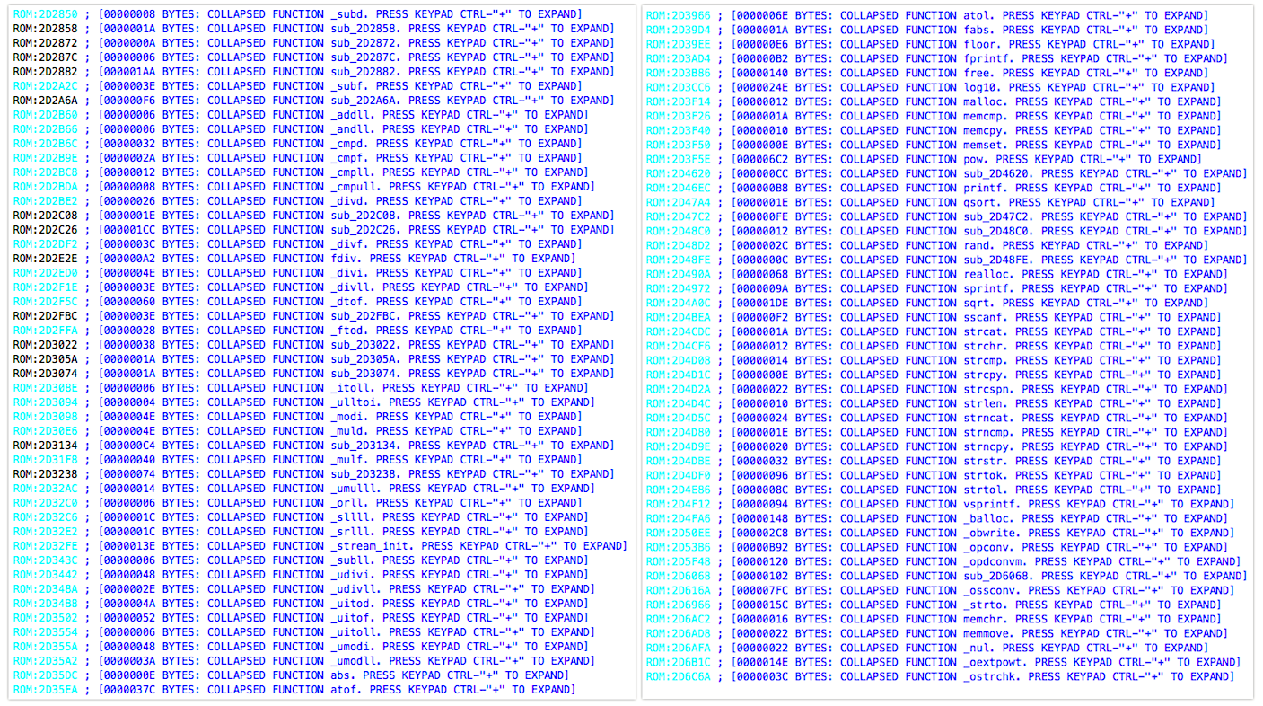
Layout
The first thing I noticed was the amount of strings in the firmware. Many functions had their names in the body or at least some indication of their behaviour. This was extremely helpful during reverse engineering in order to understand the layout.
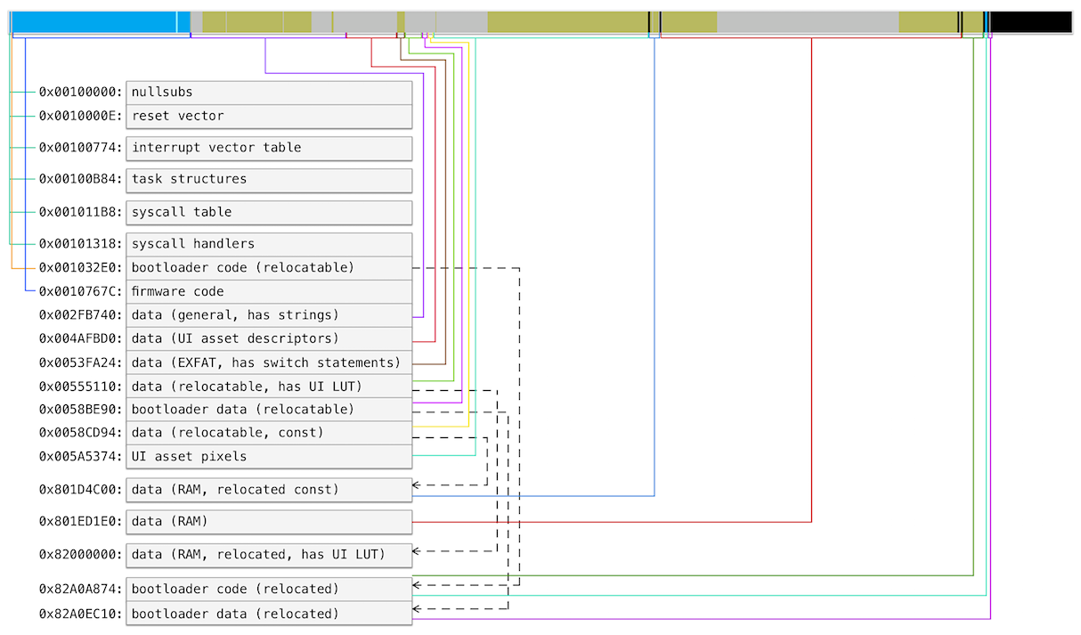
It is also important to note here that some parts of the firmware file are copied to different address in reset handler. For example, there is a bootloader embedded in code which is relocated to the higher RAM in runtime.
I had to create additional sections manually and eventually got to the following layout.
Interrupts
An interrupt vector table can be found by TBR access (Table Base Register):
   LDI:32  #int_table, R0
   MOV     R0, TBR
This usually happens in the reset vector handler right in the beginning of the firmware.
Handler addresses in the table are stored in reverse order according to formula TBR + (0x3FC - 4 × inum), so that reset vector is located at the end of the table at offset 0x3FC.
I found most of these interrupts defined in FR Hardware Manual[11] and just assumed Leica’s Maestro processor had a similar layout.
Then looking into every handler and I tried to find a string or any other hint revealing interrupt purpose.
This is what I ended up with:
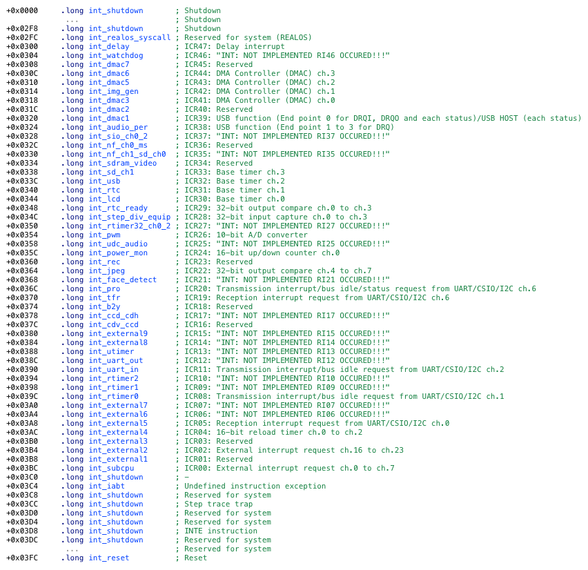
Many of these like AUDIO/SDIO/VIDEO/JPEG/RAW were expected, but can you spot the most intriguing one?
I am talking about int_uart_in, which means the camera probably has some sort of UART CLI.
Syscalls
Like pretty much any other OS, SOFTUNE REALOS is designed to use system calls for IPC and other operations.
In assembly system call looks like this:
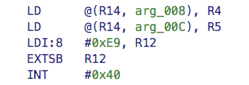
The actual address of system call hander is calculated in the following manner.
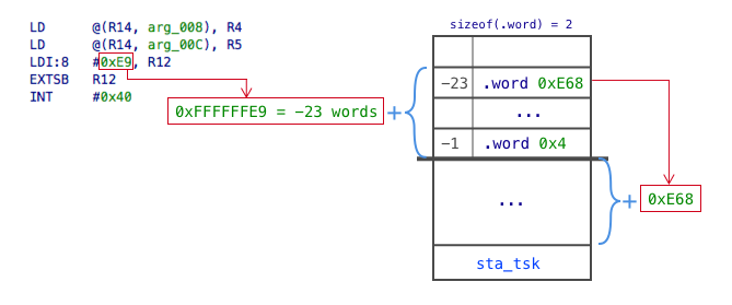
Let’s start with finding INT #0x40 interrupt handler. According to the previous section this is
(0x3FC - 4 × inum) = (0x3FC - 4 × 0x40) = 0x2FC = int_realos_syscall
Looking through the handler it is easy to find reference to the bottom of the syscall table. It contains 16bit words.
Particular entry in this table is calculated using following formula syscall_table_bottom + (num * 2):
[syscall_table_bottom + (-23 * 2)] = [syscall_table_bottom - 0x2E] = [0x1012EA] = 0xE68
As you can see this doesn’t looks like address, because the actual system call handler address is calculated as syscall_table_bottom + offset.
Following diagram shows the whole process.
All system calls and their magics are listed in SOFTUNE REALOS/FR KERNEL MANUAL[16], therefore it was possible to recover all implemented handlers in the table and improve IDB a bit further.
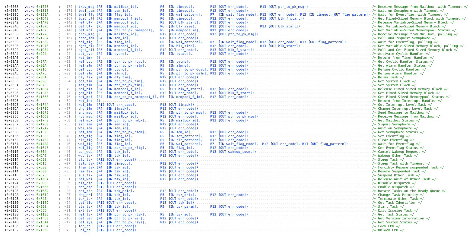
And of course, it was possible to make code even prettier defining syscall types in IDA.

I actually wrote an IDA python script to find that and some other stuff automatically[17]
Tasks
Looking at sta_tsk syscall I noticed that there is no main task function passed as parameter, instead code is passing pid. This means it was a time to look for big array of task descriptors. And it makes sense to start from sta_tsk itself.
ROM:102180 sys_sta_tsk:
ROM:102180                 ST      RP, @-R15
ROM:102182                 LDUB    @(R14, 0x4F), R3
ROM:102184                 LDI:32  #word_100B80, R14
Right at the beginning we see some reference. I had to play a bit with data types, but eventually pieces came together into this:
ROM:100B80 word_100B80:    .word 0xF           ; number of tasks
ROM:100B82                 .word 0x1C          ; task descriptor size

ROM:100B84                 .long 0x82A09F5C    ; task 1 descriptor
ROM:100B88                 .long 0x1000D
ROM:100B8C                 .long 0
ROM:100B90                 .long 0x40000000
ROM:100B94                 .long sub_1A7DB2    ; task main
ROM:100B98                 .long 0x8286EEC0
ROM:100B9C                 .long 0

ROM:100BA0                 .long 0x82A09F88    ; task 2 descriptor
ROM:100BA4                 .long 0x20010
ROM:100BA8                 .long 0
ROM:100BAC                 .long 0x40000000
ROM:100BB0                 .long sub_1A6BD2    ; task main
ROM:100BB4                 .long 0x8287EEC0
ROM:100BB8                 .long 0
...
and so on. 15 tasks in total. It was just a matter of time to look into every single main function and find the name and purpose of the task (apart from the last one). Here is the full list:
- SubCPU
This task seems to be responsible for capture operations like exposure, live view control etc. - KeyManager
Most likely this task is handling hardware buttons. - GuiManager
Pretty big task implementing UI state machine and interface drawing. - DebugManager
Yeah, there is something for debug. Yum Yum. - FileManager
This task is all about file operations. - FamManager
I would say this one is responsible for file memory because it depends of File Manager and Memory Manager tasks - MemoryManager
No surprises here, memory operations, pool control etc. - ImageManager
This task is controlling encode/decode and other image workflows - UsbManager
Current task is handling communication over USB which includes MassStorage, PTP and some Leica Custom protocol. - IOManager
Looks like this task is managing storage devices like SD and CF cards (what? CF? maybe that is what 213 board is all about). - SystemManager
Various things like general system operations, power control etc. - SettingsManager
This task is handling changes in camera state and settings. - MonitorManager
The purpose of this task is to track changes in camera state and inform other tasks. - PeripheralManager
GPS, luminance and some other sensors are controlled by this task. - Unknown
Unfortunately, I didn’t find anything relevant about this one
Interesting to note here that there is one more outstanding task descriptor after main array.
ROM:100D28 dword_100D28:   .long 0x82A0A1F0
ROM:100D2C                 .long 0x21
ROM:100D30                 .long 0
ROM:100D34                 .long 0x80000000
ROM:100D38                 .long tid16_task
ROM:100D3C                 .long 0x8285EEC0
ROM:100D40                 .long 0
And the task function is just a branch to itself.
ROM:101494 sub_101494:
ROM:101494                 BRA     sub_101494      ; CODE XREF: sub_101494
This descriptor is referenced at the end of start function which is responsible for spawning other tasks and firmware setup. So it is most likely an idle task.
Modules and Messages
Apart from tasks it was also possible to define some logical objects like IO and Peripheral modules. Modules are represented as group of message handlers within one of the tasks.
IO group seems to include:
- IO Manager
- Sub CPU
- USB Manager
- USB PTP
- USB Leica Custom
- USB Mass Storage
- Key Manager
- Debug Manager
- Lens Manager
while Peripheral group has:
- Peripheral Manager
- Luminance Sensor
- LEDs
- Beeper
- Tilt sensor
- Cover Detection
- GPS module
- 3DAxis module
Messaging system itself appears to utilise standard SOFTUNE structures:
struct RealOS_MsgPayload
{
  uint32_t msgID;   // +0x0
  uint32_t data[];  // +0x4
}

struct RealOS_Message
{
  uint32_t            os_reserved1; // +0x0
  uint32_t            os_reserved2; // +0x4

  uint32_t            to;           // +0x8
  uint32_t            from;         // +0xC
  RealOS_MsgPayload*  payload;      // +0x10
}
As expected IPC is also designed to have several message groups. Taking into consideration that there are plenty of messages handled in tasks and modules, I was able to recover just some of these groups browsing through the firmware:
0x1101xxxx - global system messages like
             0x11010002 = SYS_UPDATE_BOOTLOADER or
             0x11010005 = SYS_ERASE_SETTINGS
0x1102xxxx - messages related to image capture for example
             0x11020001 = CMD_CAP_CAPTURE or
             0x11020008 = IMAGE_STATUS_CHANGED
0x1104xxxx - playback related messages cover events like
             0x11040002 = PLY_DISABLE_PLAY_MODE or
             0x11040004 = PLY_IMAGE_READY
0x1108xxxx - various messages for PTP debugging e.g.
             0x11080002 = DBG_CHANGE_LEVEL or
             0x11080012 = DBG_WRITE_ROM_DUMP_SD
0x2201xxxx - USB PTP messages like
             0x22010108 = Camera Settings Change or
             0x22010118 = Request DebugObject
0x2202xxxx - pretty big group of SUBCPU messages including for example
             0x22020002 = E_SUBCPU_REQUEST_M_EXPOSURE_REQUEST
             0x22020015 = E_IO_SUBCPU_COMMAND_CLEANING_SENSOR
0x2203xxxx - some other debugging message
             0x22030001 = Debug String Command
0x2204xxxx - various IO messages like
             0x2204000C = Enable/Disable Mass Storage or
             0x22040012 = Reset device
0x330000xx - another big group related to UI, for instance
             0x33000001 = Key pressed
             0x33000007 = Lens connected
0x440000xx - not many info about this one, but looks like image processing group
             0x44000013 = E_IMG_CMD_CHANGE_PINFO
0x55xxxxxx - group of FAM message groups:
             0x558800xx = FAM file manager group or
             0x558888xx = FAM menu settings 1 group
0x6602xxxx - seems to be some LED control messages e.g.
             0x66020001 - Toggle LED with X Hz
             0x66020002 = Enable Continuous LED
0x6604xxxx - beeper control messages including
             0x66040001 = Beeper set or
             0x66040007 = Card full noise
0x6611xxxx - memory related debug messages
0x6622xxxx - memory related image processing messages
0x6660xxxx - some other memory related messages like
             0x66600006 = memory HISTOGRAM
             0x66600011 = memory RAWCOMP
0x771100xx and 0x77AA00xx - camera mode switch related messages
Unfortunately, many others are still unknown.
GUI
Let’s take a look again at the parts of the firmware file: CTRL_SYS-11, IMG-LOKI-212, IMG-DSP-212, IMG-FPGA-212 and IMG-LENSDATA-212.
What surprised me a bit was the absence of any GUI assets. But it must be somewhere and most likely it is embedded into IMG-LOKI-212.
One of my usual approaches to firmware reverse engineering is to recover all possible cross references. Not only from code, but in data section as well. Then I browse through them trying to find some patterns or links to known parts of code.
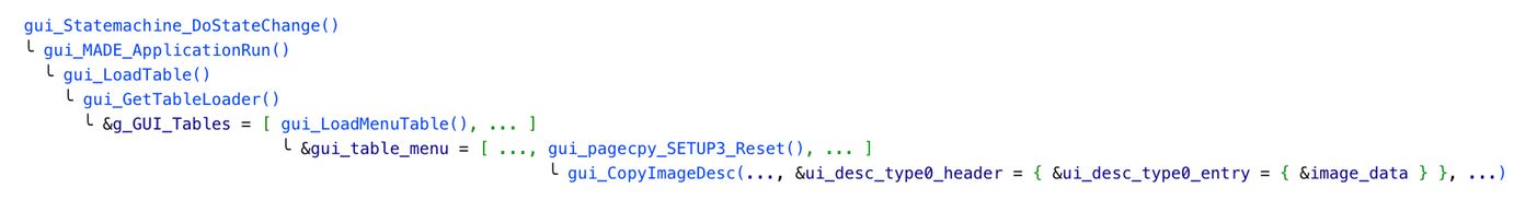
Leica firmware was not an exception. There were plenty of similar looking data sequences with addresses to data sequences with addresses to data sequences etc. Climbing up through this reference hierarchy I eventually appeared at a function I recognised.
For example, I found data structure without any references
g_data = { ... }
It was referenced from other structure
g_data_struct1 = { ... , &g_data }
Which was in turn referenced from one more structure
g_data_struct2 = { &g_data, ... }
This data structure was referenced from code and passed as parameter to another function
func1()
╰ func2(..., &g_data_struct2, ...)
However, func1() was not called directly from another function, instead if was stored in some array
g_func_list1[] = { ..., func1(), ... }
Looking above I found a reference to g_func_list1 from code
func3() {
    g_func_list1[x]
}
And again, this function was stored in array
g_func_list2[] = { ..., func3(), ... }
Array itself was referenced from some other code
func4() {
    g_func_list2[x]
}
Luckily this time function was called from another function and so on up until gui_MADE_ApplicationRun
gui_Statemachine_DoStateChange()
╰ gui_MADE_ApplicationRun()
  ╰ func5()
    ╰ func4()
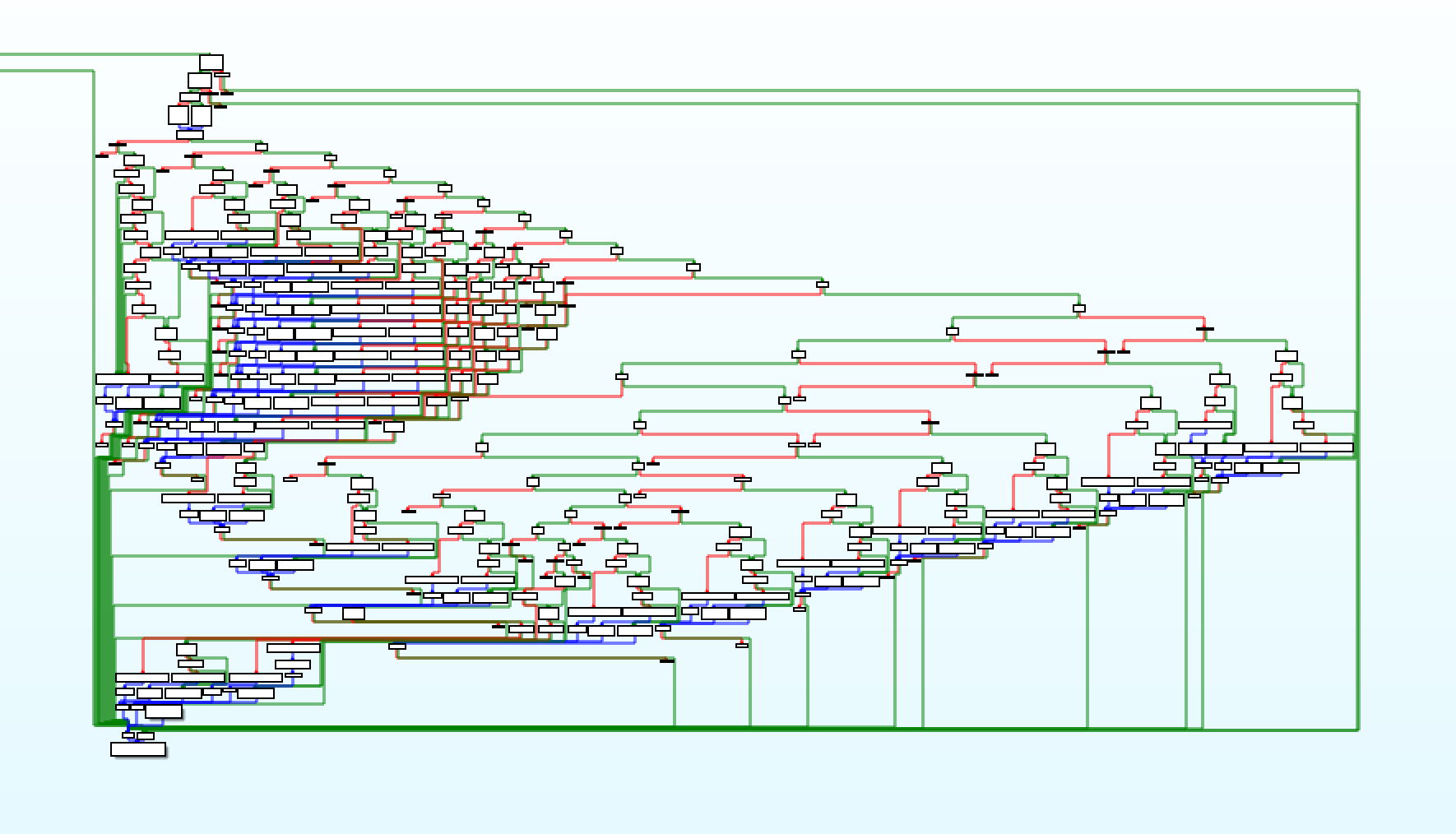
According to some strings, GUI subsystem is called “MADE” and page transitions are handled using MADE_GetSysTri whatever it means. GUI state machine is mostly implemented in gui_Statemachine_DoStateChange function. Later getting more and more information about GUI overall picture started to look like that
As you can see the core function dealing with GUI assets is gui_CopyImageDesc (it is not a real name though). It has following arguments:
gui_CopyImageDesc(
    uint32_t			dstAddress;		// R4 - destination address
    UIDescType			type;			// R5 - description type
    UITarget			target;			// R6 - rendering target
    uint32_t			descAddress;	    	// R7 - description address
    uint8_t			always0;        	// (SP + 0x0) - always 0
    uint8_t			index1;			// (SP + 0x4) - index 1
    uint8_t			index2;			// (SP + 0x8) - index 2
    uint16_t			x_offset;		// (SP + 0xC) - x offset
    uint16_t			y_offset;		// (SP + 0x10) - y offset
    uint16_t			unknown2;		// (SP + 0x14) -
    uint32_t			language1;		// (SP + 0x18) - language id 1
    uint32_t			language2;		// (SP + 0x1C) - language id 2
    uint32_t			funcAddress;		// (SP + 0x20) - function address
)
There are four types of asset descriptions:
struct UIDescType0Header         struct UIDescType1Header         struct UIDescType2                struct UIDescType3
{                                {                                {                                 {
    uint32_t    address;             uint32_t    address;             uint32_t    reg;                  uint16_t    x_offset;
    uint16_t    entries;             uint16_t    entries;             uint32_t    address;              uint16_t    y_offset;
    uint16_t    unknown;             uint16_t    unknown;             uint16_t    unknown1;             uint32_t    address;
}                                }                                    uint16_t    unknown2;         }
                                                                      uint16_t    unknown3;
struct UIDescType0Entry          struct UIDescType1Entry              uint16_t    tableoff;
{                                {                                }
    uint16_t    x_offset;            uint16_t    x_offset;
    uint16_t    y_offset;            uint16_t    y_offset;
    uint32_t    address;             uint32_t    address;
}                                    uint16_t    objects;
                                     uint16_t    total_w;
                                     uint16_t    total_h;
                                     uint16_t    unknown;
                                 }
First type has header with the reference to array of entries. Every entry has coordinates and pixel data address. Current type seems to be describing state-dependent elements, like icons which can be greyed out or disappear from the UI.
Second type also starts with header and is used for localization, describing strings or blocks of text.
Third type describes character maps for different languages.
The last type is responsible for all other static assets, like images, backgrounds etc.
Now let’s take a look at the image data itself.
+0x00: 00 08 00 14 00 01 A2 FF 0A 04 05 FF 0C 04 03 FF
+0x10: 0D 04 03 FF 0E 04 02 FF 0E 04 02 FF 04 04 06 FF
+0x20: 04 04 02 FF 04 04 06 FF 04 04 02 FF 04 04 06 FF
+0x30: 04 04 02 FF 04 04 06 FF 04 04 02 FF 04 04 06 FF
+0x40: 04 04 02 FF 04 04 06 FF 04 04 02 FF 04 04 06 FF
+0x50: 04 04 02 FF 04 04 06 FF 04 04 02 FF 0E 04 02 FF
+0x60: 0E 04 02 FF 0D 04 03 FF 0D 04 03 FF 0C 04 04 FF
+0x70: 04 04 0C FF 04 04 0C FF 04 04 0C FF 04 04 0C FF
+0x80: 04 04 0C FF 04 04 0C FF 04 04 0C FF 04 04 0C FF
+0x90: 04 04 0D FF 02 04 2D FF 00 06 00 14 00 01 79 FF
First 6 bytes look like a little header followed by some repeating pattern where every second byte is either 0xFF or 0x04.
Obvious guess for the 0x0008 and 0x0014 would be width and height in big endian. At the end of this dump we see a beginning of another sequence 00 06 00 14 00 01 which is most likely next image asset (this was also confirmed by reference to it). So the size of actual image data is 146 bytes. But the size of an image should be 0x8 * 0x14 = 0xA0 = 160. Clearly image data is not pure pixels and not even 8-bit LUT because it is 14 bytes smaller. Then what? There must be some kind of compression involved.
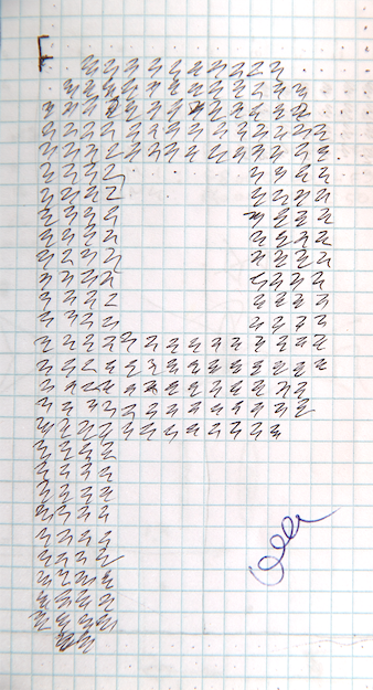
Looking at this hex dump it is hard to believe that they used something sophisticated. Also, Leica GUI is not very colourful or full of gradients and from my experience LUT is the best approach here. In this case UI assets will be full of repeating LUT indices like 03 03 03 or A1 A1 A1. Usually compressor it trying to get rid of repeating information replacing it with reference. These arrays of indices are perfect data to compress even with simple method like RLE [data][number]. In other words, write data to the output number of times.
Keeping all that in mind I assumed that this is most likely a simple image with two LUT colours (0xFF and 0x04) and the byte before colour is number of pixels to draw.
“And then you wrote another tool” you may think. Nope, I grabbed pen and paper and started to fill squares. Funny enough I still have this original drawing.
Somewhere along the way I realized that 160 pixels is not enough to fit this image, instead 0x8 and 0x14 should be multiplied by two. The third word 0x0001 is indicating if image is ASCII character so that final ImageAsset structure looks like this:
struct ImageAsset
{
    uint16_t    width;        // width/2 (big endian)
    uint16_t    height;       // height/2 (big endian)
    uint16_t    ascii;        // 1 if ASCII character
    struct      image_data {
        uint8_t number;       // number of pixels to render
        uint8_t color;        // index of pixel color in LUT
    } data[];
}
However, one part is still missing - the LUT.
It was not that hard to find one because a lot of references and structures were already recovered manually, so I was slowly scrolling through data sections looking for 256 item array of 16bit or 32bit values until I ran into this:
 .long  0x7008080, 0x72D8080, 0x73C8080, 0x75A8080, 0x79B8080, 0x71DFF6B, 0x7BE8080, 0x7FF8080
 .long  0x77BBD27, 0x75B60E7, 0x7835F4A, 0x7D3089F, 0x7018080, 0x7028080, 0x7038080, 0x7048080
 .long  0x7058080, 0x7068080, 0x7078080, 0x7088080, 0x7098080, 0x70A8080, 0x70B8080, 0x70C8080
 .long  0x70D8080, 0x70E8080, 0x70F8080, 0x7108080, 0x7118080, 0x7128080, 0x7952B15, 0x7138080
 .long  0x7148080, 0x7158080, 0x7168080, 0x7178080, 0x7188080, 0x7198080, 0x71A8080, 0x71C8080
 .long  0x71D8080, 0x71E8080, 0x71F8080, 0x7338080, 0x7208080, 0x7218080, 0x7228080, 0x7238080
 .long  0x7248080, 0x7248080, 0x7268080, 0x7278080, 0x7288080, 0x7298080, 0x72A8080, 0x72B8080
 .long  0x72C8080, 0x75E8080, 0x7608080, 0x7628080, 0x7648080, 0x7678080, 0x7688080, 0x7698080
 .long  0x76B8080, 0x76E8080, 0x7708080, 0x7728080, 0x7758080, 0x7778080, 0x7798080, 0x77C8080
 .long  0x77E8080, 0x7818080, 0x7838080, 0x7868080, 0x7888080, 0x78B8080, 0x78D8080, 0x7908080
 .long  0x7928080, 0x7958080, 0x7978080, 0x7998080, 0x79C8080, 0x79D8080, 0x7668080, 0x79E8080
 .long  0x7A18080, 0x7A28080, 0x7A38080, 0x7A68080, 0x7A78080, 0x7A88080, 0x7AB8080, 0x7AC8080
 .long  0x7AD8080, 0x7B08080, 0x7B28080, 0x7B58080, 0x7B88080, 0x7B98080, 0x7BC8080, 0x7CC8080
 .long  0x7AB3BBB, 0x7E10094, 0x7E4556E, 0x4008080, 0x2922D17, 0x7B2AB00, 0x7C2A262, 0x71DFF6B
 .long  0x768D4A2, 0x769D4EA, 0x7BD88AE, 0x705997B, 0x70BB377, 0x711CC73, 0x717E66F, 0x7238866
 .long  0x729A262, 0x72FBB5E, 0x735D55A, 0x7417751, 0x747914D, 0x74DAA48, 0x753C444, 0x75F663B
 .long  0x76B9933, 0x7998080, 0x771B32F, 0x77D5526, 0x7836F22, 0x789881E, 0x78FA21A, 0x7159095
 .long  0x71AAA91, 0x720C38D, 0x726DD88, 0x7506F6A, 0x7568866, 0x75CA262, 0x762BB5E, 0x76E5E55
 .long  0x7747751, 0x77A914D, 0x780AA48, 0x78C4D3F, 0x792663B, 0x7988037, 0x79E9933, 0x7AA3C2A
 .long  0x7B05526, 0x7B66F22, 0x7BC881E, 0x72488AE, 0x72AA1AA, 0x72FBBA6, 0x735D4A2, 0x7427799
 .long  0x7489095, 0x74DAA91, 0x753C38D, 0x77E556E, 0x7836F6A, 0x7898866, 0x78FA262, 0x79C4459
 .long  0x7A15E55, 0x7A77751, 0x7AD914D, 0x7BF4D3F, 0x7CC8080, 0x7C5663B, 0x7CB8037, 0x7337FC8
 .long  0x73999C4, 0x73FB2C0, 0x745CCBB, 0x7757799, 0x74C54FF, 0x77B9095, 0x780AA91, 0x7AB3C72
 .long  0x7B1556E, 0x7B66F6A, 0x7BC8866, 0x74277E1, 0x74890DD, 0x74EAAD9, 0x754C3D5, 0x76066CC
 .long  0x7667FC8, 0x76C99C4, 0x772B2C0, 0x77E55B7, 0x7846EB3, 0x78A88AE, 0x790A1AA, 0x7526EFB
 .long  0x75787F7, 0x75DA1F3, 0x763BAEE, 0x76F5DE6, 0x77577E1, 0x77B90DD, 0x781AAD9, 0x78D4CD0
 .long  0x79366CC, 0x79F99C4, 0x7E10094, 0x7CF44A1, 0x7DB7799, 0x7E71A90, 0x7ED338C, 0x7FF8080
 .long  0x7328080, 0x7DC8080, 0x7C88080, 0x7508080, 0x775CD2C, 0x76944EA, 0x7808080, 0x71A61FF
 .long  0x7244D40, 0x7242C15, 0xFFF8080, 0xF338080, 0xF668080, 0xF998080, 0xFCC8080, 0xF008080
 .long  0xF4C54FF, 0xFAB3BBB, 0xFE10094, 0xFE4556E, 0xF952B15, 0xFDA7751, 0xFB2AB00, 0xFC2A262
 .long  0xF1DFF6B, 0xF68D4A2, 0xF69D4EA, 0xFBD88AE, 0xA922D17, 0xC6E4130, 0xE286963, 0x74C55FF
 .long  0x768D536, 0x7FF8080, 0x7FF8080, 0x7FF8080, 0x2922D17, 0x46E4130, 0x6286963,    0x8080
Again, thanks to my work for Blackmagic Design I was able to spot YUV pixels straight away (like all these 8080 values for example).
Obviously it was insane to dump the entire UI by hand with the pen again, so yeah, I created another tool - M240UITool[18]
Leica M (typ 240) UI Tool v1.0
Usage: ./M240UITool [-a address] [-i imagebase] [-s script] [-d dump] [-f folder] [-l LUT] [-rbv] FIRMWARE.BIN

This tool will help you to find UI resources in firmware.
Use following arguments:
    -a      Specify address of the gui_CopyImageDesc function (ex. 0x2F95E0)
    -i      Specify firmware imagebase
    -s      Specify IDC file name
    -c      Specify container file name
    -d      Specify dump image format
       png  - PNG format
       bmp  - BMP (ARGB) format
    -f      Specify folder for dumped images
    -l      Specify LUT for images (filename of address)
    -b      Specify number of bytes to display in verbose mode
    -r      Try to recover string characters
    -v      Be verbose
Apart from dumping all image assets from firmware file to BMP/PNG, this tool can also produce IDC script for IDA to define all UI resources.
So far we already know that gui_CopyImageDesc is called multiple times from the function creating one UI page. I thought it would be awesome to have a UI resource browser and define all page-rendering functions. This is what the -c option is for - it produces a special container to be used in the viewer.
And who said that a UI resource browser cannot look fancy?
Being interactive (semi-transparent buttons on a screenshot above) this tool allows you to not only scroll through EVF/LCD menu pages, but also to step through rendering stages within one page.
Unfortunately, the source for this masterpiece was lost somewhere but the header files are still there as a part of M240UITool, so it is technically possible to recreate it from scratch.
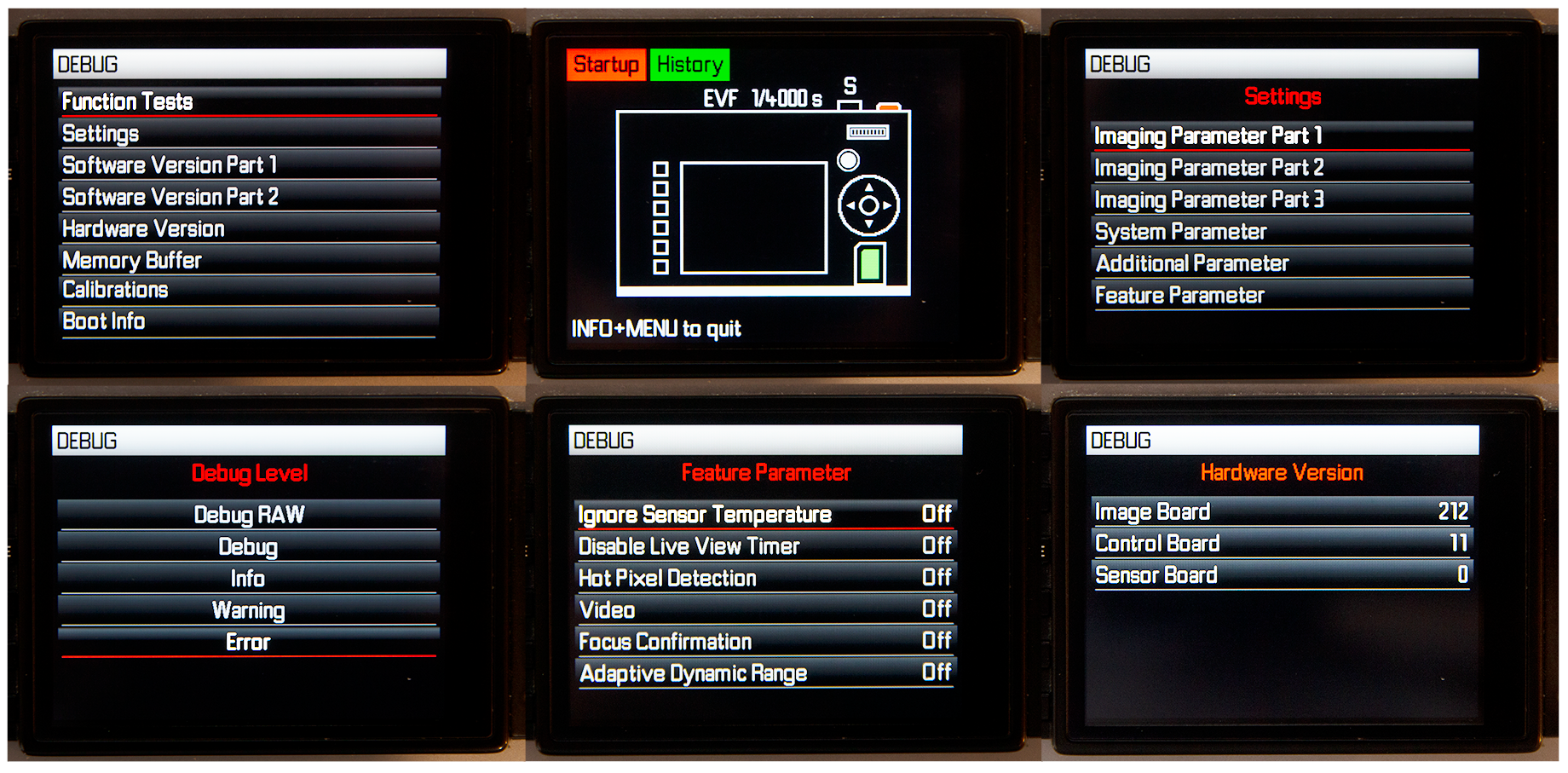
Debug Menu
What is the first string the reverse engineer usually searches for in the target? I bet on “debug” and derivatives.
There were plenty of interesting strings in firmware, but these ones are special:
$ strings ./IMG_LOKI-212_1.1.0.2.bin | grep "Debug Mode"
GUI: State: %d! Scanning for Debug Mode successful
GUI: Scanning for Debug Mode: State: %d, Ignore long DEL
GUI: Scanning for Debug Mode: State: %d
GUI: Scanning for Debug Mode: State: %d, Ignore long DEL
GUI: Scanning for Debug Mode: State: %d
GUI: Scanning for Debug Mode: State: %d, Ignore long DEL
GUI: Scanning for Debug Mode: State: %d
GUI: Scanning for Debug Mode: State: %d, Ignore long DEL
GUI: Scanning for Debug Mode: State: %d
GUI: Scanning for Debug Mode: State: %d, Ignore long DEL
GUI: Scanning for Debug Mode: State: %d
...
GUI: ScanningForDebugWithKeyAndJoyStick(): g_GUI_CheckForDebugWithKeyAndJoyStick = %d
Looks like it is possible to enter camera debug mode using some key combo. All these strings are referenced from one giant function ScanningForDebugWithKeyAndJoyStick which implements key scanning state machine. This is what it looks like in IDA
I am not going to lie, it took some time to understand how hardware buttons are handled in firmware and then to recover enums for keys and joystick. But even after I got the combo it was pretty disappointing to find out that it does nothing. Probably it works only from some particular GUI page. A couple more evenings of manual GUI state machine tracing and this problem was solved as well pointing to the Reset menu page.
Finally - Welcome to Debug Mode
I have been thinking a lot if I should make this combo public but decided not to do that. I respect the hard work Leica is doing bringing their unique cameras to market and don’t want to be responsible if their Service Centres are flooded with broken bodies as a result of some thoughtless curiosity.
Having said that, I would like to provide some enums to make reverse engineering a lot easier for someone who is willing to walk the same path.
enum ControlActionType {
    kControlAction_Idle,        // 0
    kControlAction_Push,        // 1
    kControlAction_Release,     // 2
    kControlAction_LongPush     // 3
};

enum ControlBtnType {
    kControlBtn_LV,             // 0
    kControlBtn_PLAY,           // 1
    kControlBtn_DEL,            // 2
    kControlBtn_ISO,            // 3
    kControlBtn_MENU,           // 4
    kControlBtn_SET             // 5
};

enum ControlJoystickType {
    kControlJoy_INFO,           // 0
    kControlJoy_Up,             // 1
    kControlJoy_Down,           // 2
    kControlJoy_Left,           // 3
    kControlJoy_Right           // 4
};
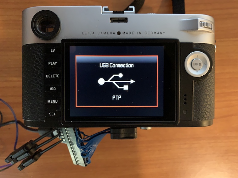
PTP
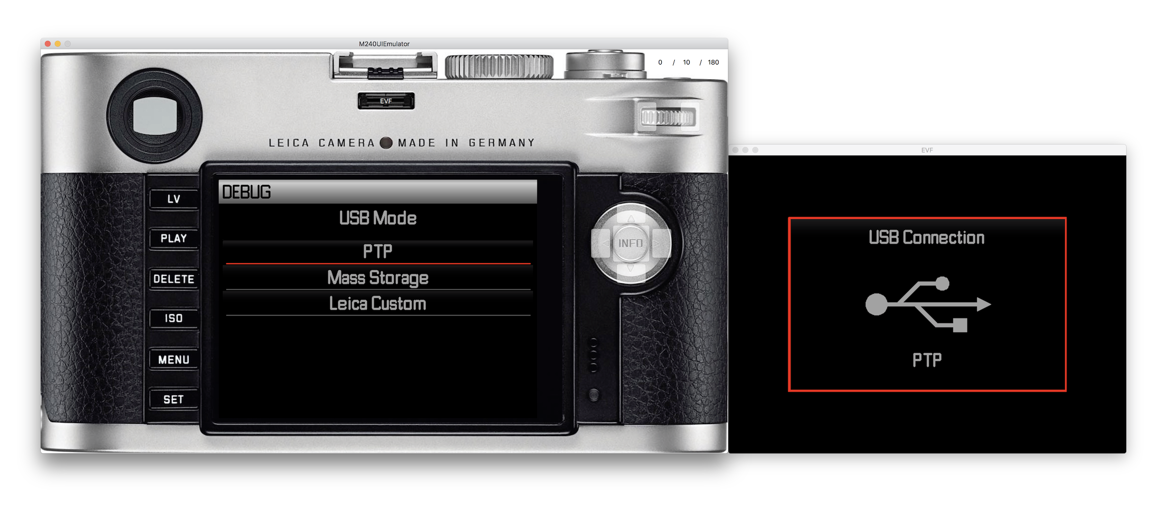
Looking around USB task code I was able to identify three different USB modes (it was also confirmed by debug menu):
- PTP
- MSC (Mass Storage Class)
- Leica Custom
PTP is the most interesting one because it is well documented and allows you to control the camera.
It is pretty easy to locate PTP handlers in the firmware because there are a lot of strings referenced from that code.
All PTP requests are divided into three groups: Legacy, Leica Extended (LE) and Production.
Debug messages helped to name pretty much every code.
Legacy:                            Leica Extented:                          Production:
0x1001 - GetDeviceInfo             0x9001 - Set Camera Settings             0x9100 - Open Production Session
0x1002 - OpenSession               0x9002 - Get Camera Settings             0x9101 - Close Production Session
0x1003 - CloseSession              0x9003 - Get Lens Parameter              0x9102 - UpdateFirmware
0x1004 - Get Storage ID            0x9004 - Release Stage                   0x9103 - Open OSD Session
0x1005 - Get Storage Info          0x9005 - Open LE Session                 0x9104 - Close OSD Session
0x1006 - GetNumObjects             0x9006 - Close LE Session                0x9105 - Get OSD Data
0x1007 - GetObjectHandles          0x9007 - RequestObjectTransferReady      0x9106 - GetFirmwareStruct
0x1008 - GetObjectInfo             0x9008 - GetGeoTackingData               0x910B - GetDebugMenu
0x1009 - GetObject                 0x900A - Open Debug Session              0x910C - SetDebugMenu
0x100A - Get Thumb                 0x900B - Close Debug Session             0x910D - ODIN Message
0x100B - Delete Object             0x900C - Get Debug Buffer                0x910E - GetDebugObjectHandles
0x100E - Initiate Capture          0x900D - Debug Command String            0x910F - GetDebugObject
0x1014 - GetDevicePropDesc         0x900E - Get Debug Route                 0x9110 - DeleteDebugObject
0x1015 - GetDevicePropV            0x900F - SetIPTCData                     0x9111 - GetDebugObjectInfo
0x101C - Initiate Open Capture     0x9010 - GetIPTCData                     0x9112 - WriteDebugObject
                                   0x9020 - Get3DAxisData                   0x9113 - CreateDebugObject
                                   0x9030 - OpenLiveViewSession             0x9114 - Calibrate 3Daxis
                                   0x9031 - CloseLiveViewSession            0x9115 - Magnetic calibration
                                   0x9033 - Unknown                         0x9116 - Get Viewfinder Data
The PTP interface implementation itself seems standard, however some commands have constrains that I intentionally omit here.
Anyway, all the above is pretty exciting, so you may think “Lets just connect camera over USB and start probing with libptp”.
Oh, shi…
Leica M240 does NOT have a USB port by design.
Handgrip Port
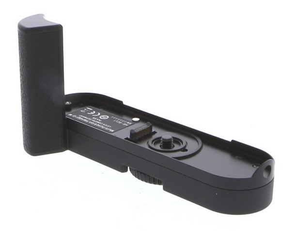
Leica doesn’t offer a lot of accessories for this camera, however there is one particularly interesting. I am talking about Leica Multifunctional Handgrip M (14495). It replaces the bottom metallic place and provides built-in GPS and several outputs like USB, SCA flash terminal, DIN/ISO-X and power sockets.
And you may think again “Awesome, let’s just buy that, attach it to the camera, connect the camera over USB and start probing with libptp”.
Oh, shi…
It costs almost $900 USD.
It is like nine hundred reasons to craft my own adapter instead. However, just in case I set up eBay notifications for used grip.
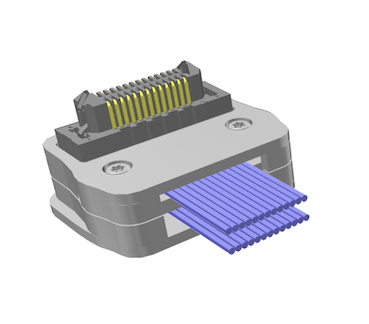
The Socket
Socket on a camera looks like this:
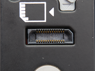
I tried searching for it on the internet, but seriously, how would you describe it to google?
Being a bit desperate I have started to think about some crazy things like gluing foil or needles to the eraser until one day at work in Blackmagic Design looking at camera PCB I have noticed that one socket has a very familiar shape. The next day I brought my Leica M240 to work and yes, it looked similar, just a lot longer with more contact pads.
So it was a matter of asking our component manager for a part number and then browsing Samtec for the one I need - ERM8-013-05.0-L-DV-TR [19]
We also asked Samtec if it is possible to get a sample and yes, they kindly agreed to send us some.
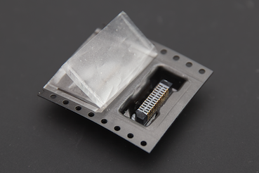
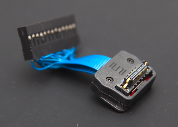
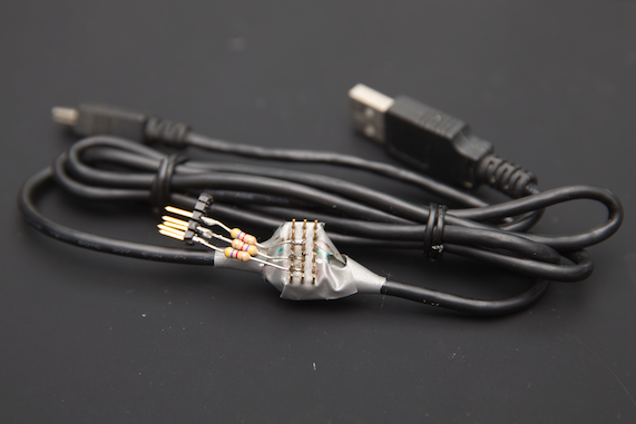
A bit of soldering, cardboard and tape to get my own breakout v2013.
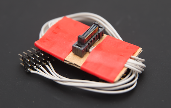
Later in 2018 I decided to ask Samtec personally for another sample. However, this time I wanted something better.
ERCD-013-05.00-TTR-TTR-1-D [20]
Then it was lots of soldering, swearing, wire cutting, swearing and soldering again just to get breakout v2018:
Pinout
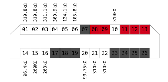
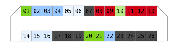
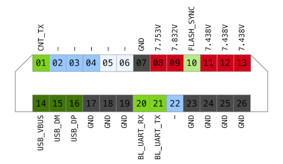
The socket has 26 contacts - 13 on each side. Even before I managed to build my breakout I have done some research probing camera socket using multimeter and logic analyser. By the way, it is necessary to put a magnet on a bottom lid sensor in order for camera to think a cover is attached.
Ground (camera is off, no battery)
I always start with the ground because it is safe and very easy to find.
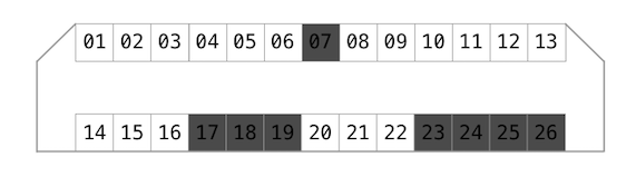
So there are 8 ground lines altogether (dark grey).
Potential (camera is on)
When the camera is ON it is possible to measure the potential on each pad in order to get an idea about logic and power levels.
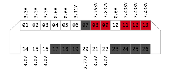
The levels on 8-9 and 11-13 are too high to be logic, therefore I defined these pads as power (red).
Resistance (camera is off, no battery)
Another useful thing to measure is resistance. In some cases it helps to identify inputs and group some lines.
Linked outputs (camera is off, no battery)
Then I have decided to probe all external contact pads on the camera body to check if they are linked to the service port.
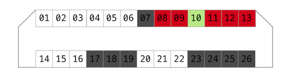
Flash Sync pad on hotshoe was directly connected to line 10.
Logic Analyser (camera is on)
Data for every line was captured using the following sequence:
Turn ON, camera should be in LV mode, take a picture, start video recording
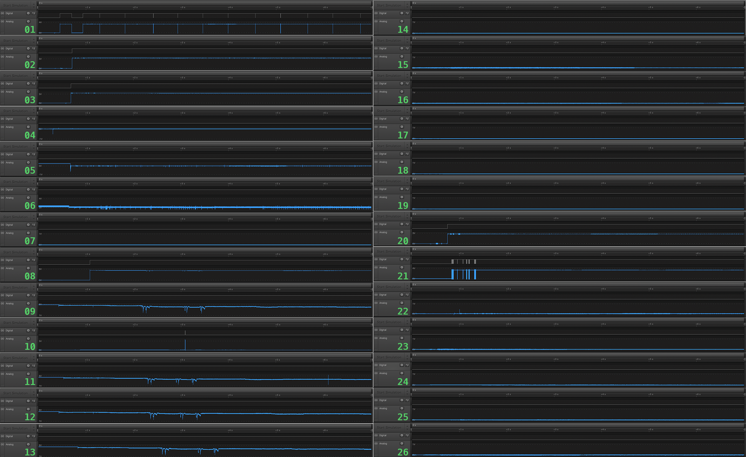
There were two lines showing some kind of data transfers: 01 and 21.
01 - 115200, 8 Bits per Transfer, 1 Stop Bit, Even Parity Bit, LSB first
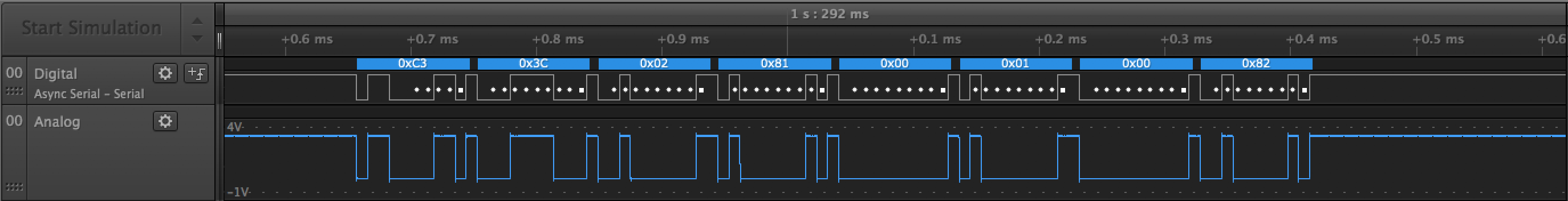 Every 500ms it sends some counter
 C3 3C 02 81 00 01 00 82, C3 3C 02 81 01 01 00 83, C3 3C 02 81 02 01 00 80 …
21 - 115200, 8 Bits per Transfer, 1 Stop Bit, No Parity Bit, LSB first
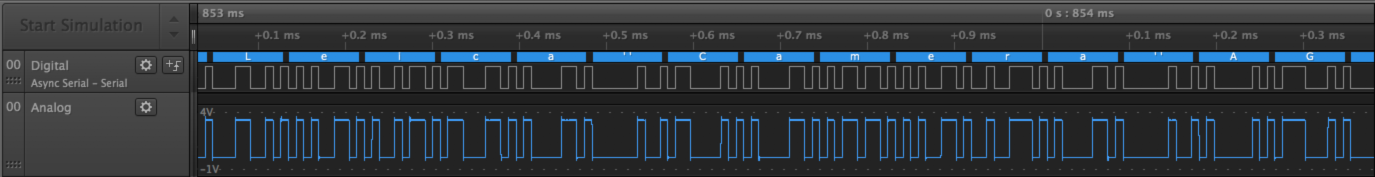 It sends SH7216 bootloader log (“Leica Camera AG” on screenshot above)
Let’s mark them with dark blue. It is pretty sad not having Maestro log exposed somewhere even with maximum debug level enabled in Debug menu.
The ones with signals have resistance around 310kOhm.
Don’t know why, but I assumed that other data lines might have similar resistance or close. Therefore, I have defined ~300kOhm, ~200kOhm and ~100kOhm lines as data as well (shades of blue on a picture).
Combined, I have the following picture.
12 candidates for data lines. But how to test that? After a brief chat with hardware people about electrical safety working with ICs, I ended up poking via 4kOhm resistor which supposed to reduce the current to a level where I am unlikely to burn inputs.
UARTs
Another assumption I made is that RX line should be next to TX line. Lines 02, 03 and 20 look like good candidates because they are both 3.3V like TX.
Initially, I used Bus Pirate to talk to these lines, but unfortunately it couldn’t keep up giving a pretty messy result. Then I switched to SiLabs based cables since they are a lot more reliable and do not conflict with anything on macOS.
At first, I attached cable TX to pin 20 and started to type help after bootloader banner. As expected the camera echoed characters back after a short delay.
The next UART looking pins are 02 and 03. Unfortunately, there was no indication that someone is listening on those.
On a diagram known UARTs are defined with darker shade of green.
USB
It all started with a cut in half USB cable with header in a middle and 4kOhm resistors to probe. Signal integrity for differential pair? Nah, it didn’t bother me much back then :)
Then I sniffed some consumer devices with USB at home to get an idea what USB comm looks like.
Canon Camera

Blackmagic Pocket Cinema Camera

Canon Camcoder

JVC Camcoder

Keyring

KidiZoom Camera

They are all a bit different, but initial D- D+ state is low. Well, good to know, let’s check what is left on grip port similar to that:
22 - unlikely because D- D+ are differential pair and should be pretty close
04/05 - unlikely because they have different resistance
14/15 - unlikely because they have different resistance
15/16 - possible because they are close and have similar resistance
Therefore, I attached USB D- D+ to the 15/16 and plugged it to iMac…
There was USB PTP on a screen, but camera still didn’t appear on the host. I tried setting up various USB termination schemes on breadboard but nothing worked. Beagle showed many corrupted packets and other errors. Eventually I gave up and got back to reverse engineering firmware.
This is the final pinout with USB painted as dark green.
Who would have thought, several years later I received desired eBay notification and managed to get this grip pretty cheap.
Finally, I could check my PTP findings. But first I was obviously curious what does USB PHY look like inside the grip.
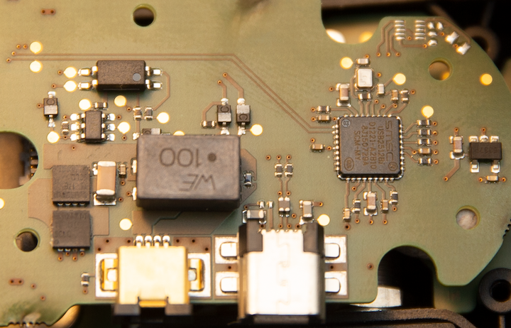
Inside I found SMSC 2512b hub[21] right on the way from grip socket to Mini USB connector. Chip is operating in default mode because there is no EEPROM and SCL/SDA pins are pulled down. First downstream port is routed to the camera body socket, but second one is not connected to anything.
I am probably missing something but to me this solution doesn’t make a lot of sense. Looking through datasheet I found out that chip has “Fully integrated USB termination and Pull-up/Pull-down resistors”. Maybe Leica engineers decided not to implement their own USB PHY and used the one in a hub which is very well tested and works out of the box. Actually, I can’t blame them because I tried to do same myself earlier and it seems to be a tricky task. It can also be a feature protecting grip from counterfeit, who knows.
Anyway, if you are good at USB PHY and willing to help, feel free to ping me, it should be possible to make USB port work without grip :)
PTP again
As I have said it was time to play with Leica PTP extensions.
Luckily I found pretty cool C++ library to use instead of libptp - libEasyPTP[22]. It also didn’t take long to write tool based on this library since I already knew some constrains in Leica PTP interface.
An even if M240PTPTool is quite buggy it was good enough as PoC[23].
There are just two PTP requests used: GetDebugBuffer (0x900C) and DebugCommandString (0x900D).
By the way, in order to make modules to fill debug log it is necessary to set Debug Level to “Debug” or “Debug RAW” in Debug Menu.
Tool CLI provided several options:
exit quits the tool;
flush command dumps debug buffer from the camera:
M240> flush
I:[00:11:468]|01| DATE/TIME CORRECTED by 5921 sec
D:[00:12:079]|00| Send message from TID 0 to TID 1 over MBX 3 - length: 4 - MesgID: 0x22020103
D:[00:12:179]|00| Send message from TID 0 to TID 1 over MBX 3 - length: 4 - MesgID: 0x22020103
D:[00:12:282]|11| Message received from TID 0 for TID 1 over MBX 3
D:[00:12:283]|11| Message received from TID 0 for TID 1 over MBX 3
D:[00:12:301]|00| Send message from TID 0 to TID 1 over MBX 3 - length: 4 - MesgID: 0x22020103
D:[00:12:402]|00| Send message from TID 0 to TID 1 over MBX 3 - length: 4 - MesgID: 0x22020103
D:[00:12:502]|00| Send message from TID 0 to TID 1 over MBX 3 - length: 4 - MesgID: 0x22020103
...
any other text will be sent as Debug Command String to the camera. help for example outputs all possible commands with arguments:
M240> help
 ********* debug command description ********

 exposure request
 Description: requests a release from Sub CPU
 Parameter 1: Exposure Time TV

 still request
 Description: simulates the -still request- command flow of Sub CPU
 Parameter: no

 ...

 send Message;[Parameter1];[Parameter2];[Parameter2];...;...
 Description: Sending Message to Task
 Parameter 1: Receiver Task ID
 Parameter 2: Command ID
 Parameter 3: Command Data[0] (32 Bit)
 Parameter 4: Command Data[1] (32 Bit)
 Parameter 5:   .
 Parameter 6:   .
 use maximum 10 Parameter

 ...
The complete list is quite big, but wow, we can send raw Softune messages to any task! What is so interesting we could have sent there…
The other popular string to search in firmware - “dump”. Let’s take a look what we have got in our case.
$ strings IMG_LOKI-212_1.1.0.2.bin | rg -i dump
GUI: HEX DUMP: Address: %x, Length: %d
HSK: DBG_WRITE_ROM_DUMP_SD: File was properly opened, but it seems to be empty.
ROM_DUMP
HSK: DBG_WRITE_ROM_DUMP_SD: Flushing Dump to ROM. Size %d
SD:\ROM_DUMP.bin
HSK: DBG_WRITE_ROM_DUMP_SD Command received!
ROM_DUMP.bin
HSK: DUMP failed, no cards inserted!
HSK: DUMP FlashROM to SD card.
HSK: DUMP FlashROM to CF card.
Dumping files to card
Apparently, it is possible to dump firmware to SD card. It is easy to find code responsible for that by reference to string “Dumping files to card”. It is located in giant message hander of System Task (pid 11 as we already know) and can be triggered by message 0x11080006 without arguments.
Type send Message;11;0x11080006 in M240PTPTool, hit enter and observe the screen.
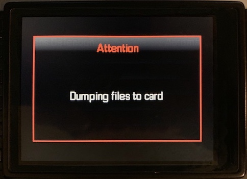
Then remove SD card and check what is on it.
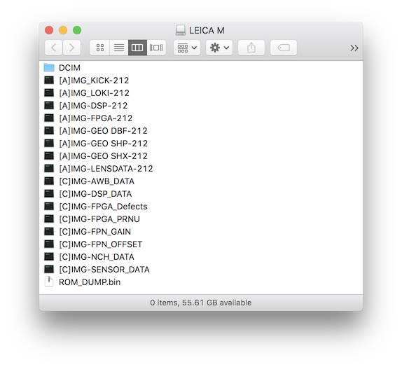
Here it is, full dump including firmware.
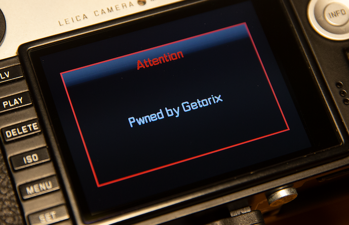
But what is more important, is it now possible to modify this firmware in any way and flash it back to camera using another debug command: send Message;11;0x11080012.
As you can see this opens up endless opportunities. For example, it should be possible to build tiny device with MCU supporting USB host and some buttons to perform complex message sequences via PTP. And if it is not enough - just flash camera with your own custom firmware…
And then we had our second child :)
Epilogue
There is usually a way to study devices you don’t want to break without opening body or soldering wires to its PCB. Below are my tips if you don’t mind:
- get all the public information you can about the device: datasheets, tear downs, internal photos, videos from factory [24] ;)
- dig into firmware if you have it in order to find hints about external outputs
- always google for various magics and odd byte sequences you find in firmware files
- measure GND/Potential/Resistance for all unknown exposed external pads
- probe these pads with logic analyser
- always remember about safety measures dealing with electronics
- try to exclude pads not in your scope of interest (ground, power)
- if you can’t recognize signal by its analogue view, try googling for the most popular ones (USB/UART/SPI/I2C/1Wire)
- if you have some ideas about signal nature, try verifying yourself with similar consumer electronics
- think
threefive times before trying to SEND data to device, like driving line low/high - and of course, do not hesitate to ask other people
@getorix | github.com/alexhude
Happy Hacking!
References
[1] https://github.com/alexhude/LeicaHacks/tree/master/Tools/pwadsplit
[2] http://doom.wikia.com/wiki/WAD
[3] https://en.wikipedia.org/wiki/LHA_(file_format)
[4] https://github.com/CatacombGames/CatacombArmageddon/blob/master/LZW.C
[5] https://github.com/krater/Blackfin-IDA-Pro-Plugin
[6] https://github.com/alexhude/LeicaHacks/tree/master/Tools/xortool
[7] https://en.wikipedia.org/wiki/List_of_file_signatures
[8] https://github.com/alexhude/LeicaHacks/tree/master/Tools/M240FwTool
[9] https://github.com/alexhude/LeicaHacks/tree/master/Tools/fr (requires IDA 6.4 SDK)
[10] https://en.wikipedia.org/wiki/Delay_slot
[11] https://edevice.fujitsu.com/fj/MANUAL/MANUALp/en-pdf/CM71-10158-1E.pdf (link is dead)
[12] https://en.wikipedia.org/wiki/Softune
[13] https://en.wikipedia.org/wiki/Relocatable_Object_Module_Format
[14] https://github.com/alexhude/LeicaHacks/tree/master/Tools/FRLibTool
[15] https://github.com/alexhude/LeicaHacks/tree/master/IDA/signatures/
[16] https://www.fujitsu.com/downloads/MICRO/fma/pdfmcu/resofrke-cm71-00321-3e.pdf
[17] https://github.com/alexhude/LeicaHacks/tree/master/IDA/scripts/softune.py
[18] https://github.com/alexhude/LeicaHacks/tree/master/Tools/M240UITool
[19] https://www.samtec.com/products/erm8-013-05.0-l-dv-tr
[20] https://www.samtec.com/products/ercd-013-05.00-ttr-ttr-1-d
[21] https://www.microchip.com/wwwproducts/en/USB2512B
[22] https://github.com/TrueJournals/libEasyPTP
[23] https://github.com/alexhude/LeicaHacks/tree/master/Tools/M240PTPTool
[24] https://youtu.be/p4t-OVIvuy8?t=196